In order to pursue our goals of next-generation detector and instrument development, we are building new tools and new test and measurement capabilities to help characterize semiconductor devices at cryogenic temperatures.
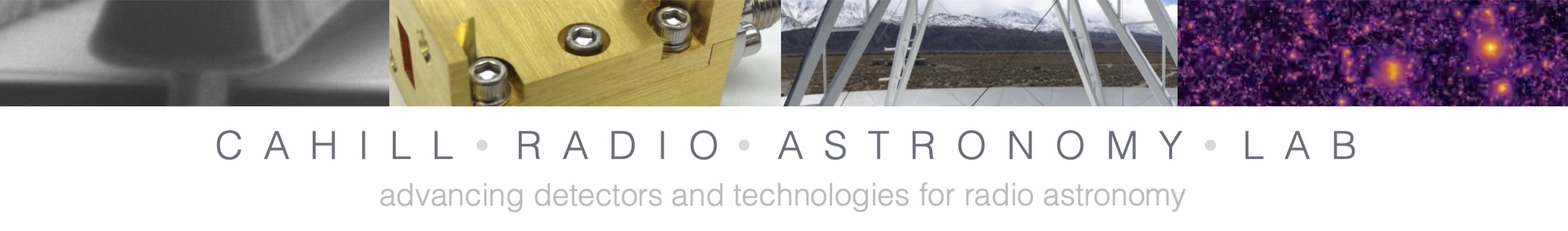
Characterizing individual HEMT low noise amplifier chips is an expensive and time-consuming process. The devices must be packaged in a brass housing along with RF/DC connectors and bias electronics. They must then be cooled to temperatures near 20 K in a cryostat with appropriate radio-frequency and DC feed-throughs. To speed up this process and allow large numbers of devices to be rapidly characterized, we developed a cryogenic wafer probe station, initially designed to operate at 75-115 GHz. This has since been modified to allow lower-frequency operation (<20 GHz) for device modeling and parameter extraction. The innovative design includes a large, 3-inch diameter wafer chuck, every part of which can be moved to the probes, in order to reduce calibration error arising from large probe movements. More recent upgrades include the ability to measure S-parameters and noise in a single cool-down, and pulsed DC biasing.
Damon Russell, Kieran Cleary, and Rodrigo Reeves , Cryogenic probe station for on-wafer characterization of electrical devices, Review of Scientific Instruments, vol. 83, no. 4, 044703-044703-10, April 2012. doi:10.1063/1.3700213
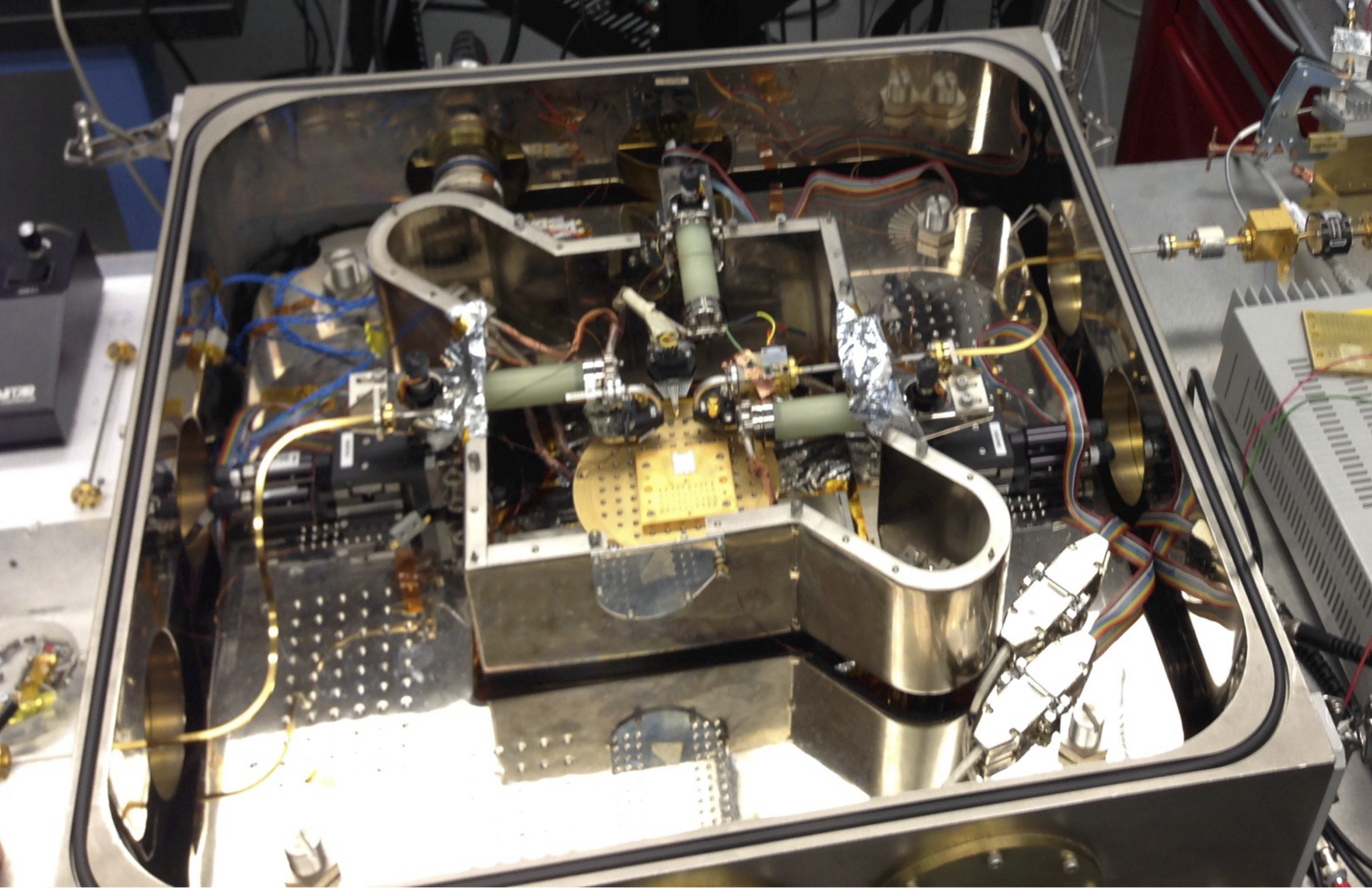
We have developed a programmable, fast switching, accurate, and miniaturized calibration load for use in millimeter and submillimeter low-noise amplifier characterization, and Earth/planetary science radiometers. The proposed solution uses a thermally conductive waveguide vane attenuator with low thermal mass, integrated heater, and silicon thermometer. The choice of cryogenically suitable materials coupled with detailed thermal analyses and proper miniaturization facilitates a programmable calibration load with a switching speed of ≲10 s. The W-band design operates over-moded to ~230 GHz, but the concept is in principle scalable to terahertz frequencies.
Jacob W. Kooi, Rodrigo A. Reeves, Arthur W. Lichtenberger, Theodore J. Reck, Andy K. Fung, Sander Weinreb, James W. Lamb, Rohit S. Gawande, Kieran A. Cleary, and Goutam Chattopadhyay, A Programmable Cryogenic Waveguide Calibration Load With Exceptional Temporal Response and Linearity, IEEE Transactions on Terahertz Science and Technology, vol. 8, no. 4, pp. 434–445, July 2018. doi:10.1109/TTHZ.2018.2826838
Supported by the National Institute of Standards and Technology (NIST) we are developing a microfabricated, wideband, on-chip resistive noise source with ultrafast response time and working temperature range from 20 K to ~ 600 K. (Work in progress)
Supported by the National Institute of Standards and Technology (NIST), we are developing a microfabricated, wideband impedance tuner based on the mismatched impedance line method, which enables fast impedance variation with frequency. (Work in progress)
Interior of the Caltech cryogenic probe station, showing three probe arms, and 'wafflepack' containing chips for measurement and calibration substrate.
Interior of fast-switching waveguide vane load (Kooi et al. 2018)